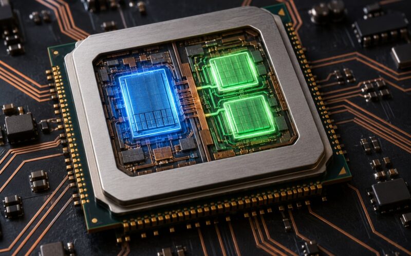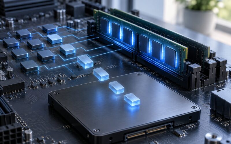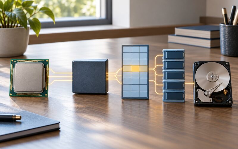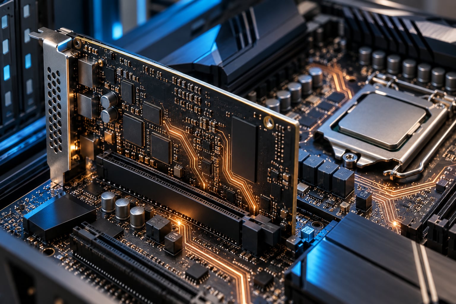
PCI Express is a high-speed serial interconnect that gives each device its own dedicated copper link to the CPU, instead of making hardware share one bus. Data moves as small packets across those links at speeds that double roughly every generation, and the link speed plus the number of lanes are negotiated automatically when the machine boots. That is the whole idea, and everything below is just the detail.
Once you have that mental model, most of the confusing parts of a motherboard spec sheet stop being confusing. A graphics card labelled “PCIe 4.0 x16” tells you two separate things: which generation the link negotiated, and how many lanes it got.
Table of Contents
- What Is PCI Express and Why Does It Matter?
- PCI, PCI-X and AGP: where PCIe came from
- How PCI Express Works: The Path Data Takes
- PCI Express Lanes and Links Explained Simply
- What “x16 (x4 mode)” actually means
- What Does PCI Express Speed Mean?
- GT/s vs GB/s: where the speed goes
- PCI Express Packet Flow: From Request to Response
- How PCIe Devices Connect to the Computer
- How PCI Express Handles Interrupts and Power Management
- Why PCIe Performance Is Usually Lower Than Advertised
- Common PCIe problems and quick fixes
- A Simple PCI Express Example: Adding an NVMe SSD
- How to check your own PCIe generation and lane count
- Frequently Asked Questions
- Is PCI Express a network connection?
- Why does a PCIe slot say x16 but the device use only x4?
- What is the difference between PCIe generation and lane width?
- Can a PCIe graphics card work in an x8 slot?
- Does PCIe bandwidth determine how fast an SSD or GPU feels?
- How do I check which PCIe link a device is using?
- What to Remember
What Is PCI Express and Why Does It Matter?
PCI Express (PCIe) is the standard bus that connects add-in hardware inside a computer to the rest of the system. The PCIe 1.0 specification was published in 2004, and the standard itself is owned and maintained by PCI-SIG, an industry consortium that also owns PCI, PCI-X and AGP.
In practice, PCIe is what carries a graphics card, an NVMe M.2 SSD, a 10GbE network card, a Wi-Fi module, a USB controller, a sound card and a video capture card. If you have ever wondered why a machine feels slow with one component and fast with another, the answer is often sitting on a PCIe link.
The interface is described as point-to-point because there is no shared bus any more. Every device talks to its own link, and where a hub is needed, a PCIe switch fans one upstream link out to several downstream ones.
PCI, PCI-X and AGP: where PCIe came from
Before PCIe, expansion cards shared a parallel bus. The lines were shared, the whole bus ran at the speed of the slowest device on it, and the CPU had to arbitration for every transfer. Timing skew across many parallel wires made high clock rates impossible to scale.
| Standard | Era | Topology | Peak bandwidth |
|---|---|---|---|
| PCI (32-bit) | 1993 | Shared parallel bus | 133 MB/s |
| PCI-X | 1999 | Shared parallel bus, server-focused | 1.07 GB/s |
| AGP | 1997 | Dedicated graphics port, parallel | 2 GB/s |
| PCI Express 1.0 | 2004 | Point-to-point serial | 250 MB/s per lane per direction |
PCI cards are still physically present on a few server and industrial motherboards, and PCI-X survives in some legacy storage controllers. Neither is in a normal desktop today.
How PCI Express Works: The Path Data Takes
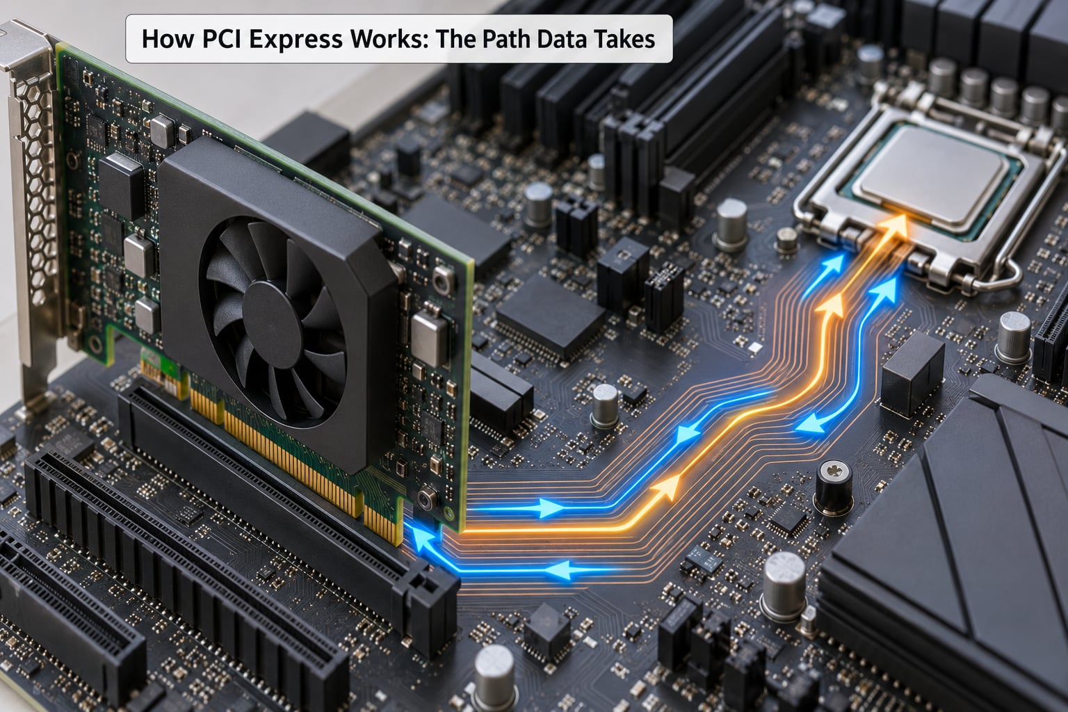
Say a GPU wants to read a texture from system memory. It cannot reach memory directly. Memory is owned by the CPU, so the request has to travel to the CPU side of the bus, get turned into a memory read, and carry the data back.
- The GPU’s controller builds a transaction, a small structured request such as “read 256 bytes at address X”.
- That transaction is packaged into packets called TLPs, transaction layer packets, with a header, optional data payload and a checksum.
- Each packet is split into smaller units and spread across the lanes of the link. With an x16 link, a packet is striped across all 16 lanes and reassembled at the far end.
- Each lane serialises its share into a stream of symbols and drives it across two copper wires as a differential pair.
- The CPU-side root complex receives the packets, routes the memory request, and sends the returned data back down the same link.
Two details make the physical layer work at all. The receiver recovers the clock from the data stream itself, which is why PCIe links can change speed at runtime and why no separate clock wire crosses the board. And the receiver checks every packet with a CRC, so a corrupted transfer is detected and retried instead of silently delivered.
PCI Express Lanes and Links Explained Simply
A lane is two differential pairs, which means four wires. One pair carries data from endpoint A to endpoint B, the other carries data in the opposite direction, so every lane is full duplex and both ends can transmit at the same instant.
Lanes group into links, and the link width is written as x1, x2, x4, x8 or x16. An x16 link is sixteen lanes working together, not sixteen separate slots; they are one link with sixteen times the bandwidth and the same latency.
Width is decided by the port on each side, and it is negotiated at power-on. If the far end only offers x8, an x16 card comes up as x8 with no error and no warning on screen. If a lane fails its training check, the link down-configures by dropping lanes, which is a designed fault-tolerance behaviour rather than a bug.
What “x16 (x4 mode)” actually means
Motherboards size the slot mechanically, and the length of the slot has almost nothing to do with how many lanes are wired to it. That mismatch is the single biggest source of confusion in the PCIe world, because marketing photos show slot length and people read it as lane count.
| Spec sheet notation | Physical slot | Electrical lanes | Usual source of the lane limit |
|---|---|---|---|
| PCIe x16 | Full length | 16 | Direct CPU attachment |
| PCIe x16 (x4 mode) | Full length | 4 | Chipset uplink, or lanes shared with M.2 slots |
| PCIe 2 x16 (x8 mode) | Full length | 8 | Second slot wired through the chipset |
| PCIe x4 | Short | 4 | Dedicated M.2 or adapter slot |
Adding an M.2 NVMe drive often takes lanes away from a slot on the same board. Read the manual’s lane-sharing table before you assume two slots will both run at full width.
What Does PCI Express Speed Mean?
Two numbers describe a PCIe link and they multiply. The generation sets the per-lane signalling rate in gigatransfers per second, and the lane width sets how many lanes run in parallel. So x16 Gen 5 is far quicker than x8 Gen 4, because it has twice the lanes and twice the per-lane rate.
| Generation | Year | GT/s per lane | Line coding | Usable GB/s per lane per direction |
|---|---|---|---|---|
| 1.0 | 2004 | 2.5 | 8b/10b | 0.25 |
| 2.0 | 2007 | 5 | 8b/10b | 0.50 |
| 3.0 | 2010 | 8 | 128b/130b | 0.99 |
| 4.0 | 2017 | 16 | 128b/130b | 1.97 |
| 5.0 | 2019 | 32 | 128b/130b | 3.94 |
| 6.0 | 2022 | 64 (PAM-4) | FLIT with FEC | 7.56 |
| 7.0 | 2025 spec | 128 (PAM-4) | FLIT with FEC | about 15.1 |
That is the “doubles each generation” rule in its most quotable form: each new generation roughly doubles per-lane bandwidth over the one before it.
| Link width | Gen 3 | Gen 4 | Gen 5 | Gen 6 |
|---|---|---|---|---|
| x1 | 0.99 GB/s | 1.97 GB/s | 3.94 GB/s | 7.56 GB/s |
| x4 | 3.94 GB/s | 7.88 GB/s | 15.75 GB/s | 30.2 GB/s |
| x8 | 7.88 GB/s | 15.75 GB/s | 31.5 GB/s | 60.5 GB/s |
| x16 | 15.75 GB/s | 31.5 GB/s | 63 GB/s | 121 GB/s |
GT/s vs GB/s: where the speed goes
GT/s counts symbols on the wire. GB/s counts payload bytes that reach the device, and the two are never equal because the link spends some of its capacity making the transmission reliable.
Gen 1 and Gen 2 use 8b/10b encoding, which turns every 8 data bits into 10 line symbols so the receiver can stay in sync. From 5 gigatransfers per second you get 4 gigabits of payload, or 500 MB/s, and you have given up 20 percent of the wire to framing. Gen 3 onwards uses 128b/130b, a much cheaper scheme that gives back about 98 percent of the wire.
Retail listings also quote the raw number in a way that flatters it. A “63 GB/s” card label is the Gen 5 x16 figure counting both directions of a full-duplex link; usable bandwidth in one direction is about 31.5 GB/s before any protocol overhead. Read the spec sheet, not the badge.
PCI Express Packet Flow: From Request to Response
Every transfer is a request and, when data is involved, a completion. Nothing is a raw stream; PCIe only ever moves defined packets.
A read request carries a requester ID, a tag, an address, a length and a requester credit count. Credits matter because the sender may only transmit as many packets as the receiver has advertised room for, which is the flow control that stops a fast endpoint from flooding a slower one.
For an NVMe read of one sector, the sequence is roughly:
- The SSD’s controller builds a memory read request TLP and sends it upstream.
- The root complex routes it to the memory controller.
- Memory returns the 4 KB of data, which is split into completion packets with data payloads, striped across the lanes.
- Each packet carries a sequence number so the receiver can reorder and reassemble, and a CRC for error detection.
- Completion status arrives, the host driver sees the request is done, and an MSI interrupt tells the CPU a completion is waiting.
Notice that nothing polls. The device raises an interrupt when it has work or has finished work, which brings us to the two systems that keep a PCIe link civilised.
How PCIe Devices Connect to the Computer
Everything PCIe hangs off the root complex, the hub inside or beside the CPU that owns memory. It contains the host bridge, one or more root ports, and the routing logic that decides whether a packet goes to memory, to another device, or out to the chipset.
A PCIe switch adds downstream ports so one upstream link becomes several independent links. That is how a four-drive NVMe card works: a small controller presents x4 to the motherboard and fans it out to four x4 endpoints behind it, and each drive runs at full speed instead of sharing one link.
Bifurcation is the related idea used in the other direction. If the CPU and board support it, a single x16 connection can be split into four independent x4 links, letting one slot carry four NVMe drives with no switch chip at all. The divider has to be supported on both ends, so you cannot just assume a slot will bifurcate.
The CPU has a fixed lane budget, usually 20 to 24 lanes, which is why lanes get shared. Chipset-attached slots draw from the same upstream link, so a second x16 slot on many boards is physically long but electrically x4 or x8.
PCIe also travels outside the case. OCuLink carries a full PCIe x4 link over a cable, and Thunderbolt and USB4 tunnels PCIe over their own link. That is how external GPU and NVMe enclosures work, with the usual caveat that the tunnel adds latency and shares bandwidth with other traffic on the same port.
How PCI Express Handles Interrupts and Power Management
Interrupts are how a device says “I need the CPU”. Older cards use a shared INTx line, so four legacy interrupts share one pin and the operating system has to work out which device fired. MSI and MSI-X replace that with a memory write that carries the device identity in the data itself, which is faster and scales to many more devices. Modern GPUs and NICs use MSI-X with a table of entries per device.
On the power side, PCIe defines a set of link power states so an idle port stops burning power without needing the whole system to sleep.
| State | What happens | Wake-up cost |
|---|---|---|
| L0 | Full speed, all lanes active | None, this is the working state |
| L0s | Unidirectional idle, quick to recover | Very low, microseconds |
| L1 | Low power idle, reduced signalling | Low |
| L1SS | Substate of L1 for primary clock-gated links | Low |
| L2 / L3 | Deep sleep, links powered down | Wake event or power on required |
ASPM, the Active State Power Management feature, decides which of these states an unused link is allowed to drop into. ASPM is partly a latency-versus-power trade you can control in firmware or the operating system, which is a common source of stutter complaints on older platforms.
Slot power is separate from the data lanes. A PCIe slot delivers a modest amount of power on its edge connector, and a card that needs more draws it from auxiliary connectors, typically 6-pin or 8-pin, with 12VHPWR and the revised 12V-2×6 on current high-end graphics cards. If a card works at idle but faults under load, a power connector that is not fully seated is one of the first things to check.
Why PCIe Performance Is Usually Lower Than Advertised
The link rate is a ceiling on the wire, not a promise about application speed. Several things sit between the two.
Encoding overhead removes bits, packet headers add overhead on every transaction, and credit-based flow control can leave a link idle while it waits for credit. Shared lanes divide one connection between two devices. Then there are the ordinary bottlenecks: a drive that cannot source data quickly enough to fill the pipe, a CPU-side bottleneck in the driver or the host bridge, and thermal limits that hold a card at a lower speed under sustained load.
The gap is easiest to see on storage. A PCIe 3.0 x4 link has about 3.94 GB/s of usable bandwidth per direction, and a good NVMe drive of that era tops out a little below that in sequential tests. The drive is the limit, not the link.
Common PCIe problems and quick fixes
- Link trains at the wrong speed. Check BIOS settings for the slot and for Above 4G Decoding, and confirm the card itself supports the generation you expected.
- Fewer lanes than expected. This is usually a physical limitation or a shared M.2 slot. The board manual’s lane table settles it.
- Device shows as x16 but reports running at reduced width. Reseat the card, clear CMOS, and check for a bent or dirty contact.
- “No PCIe bus” or resource errors in Device Manager. Add the hardware yourself in Device Manager rather than letting Windows scan for it.
- Random crashes under load. Test with the card removed to confirm it is the card, and check auxiliary power seating before anything else.
Thread after thread on r/buildapc and Tom’s Hardware arrives at the same conclusion: lane negotiation happens automatically at boot, and down-training on a bad lane is the system protecting you, not a fault you need to fix.
A Simple PCI Express Example: Adding an NVMe SSD
Here is everything above in one story. You slot a four-lane NVMe M.2 drive into a motherboard M.2 socket and boot.
At power-on, the drive’s controller and the socket begin link training. They exchange training sequences, agree on the generation both support, run equalization on each lane’s channel, and settle on a link. If the socket is wired for four lanes, the link comes up x4; if it is wired for two, it comes up x2 and the drive still works.
Enumeration follows. The system’s firmware walks the topology from the root complex, finds the new endpoint, assigns bus and device numbers, reads its BARs to learn what memory and I/O space it wants, and hands it to the operating system. The NVMe driver loads, sets up its queues, and the drive is online.
From then on, a read is a set of requests up the x4 link and completions back down, with MSI-X interrupts when work finishes. If the drive were a Gen 4 part in a Gen 3 machine, the link simply comes up at 8 GT/s per lane and everything works.
How to check your own PCIe generation and lane count
On Windows, open Device Manager, expand Display adapters or Storage controllers, right-click the device, choose Properties, then Details. Set the property to “Location information” or open the Hardware Ids tab and read the negotiated link. CPU-Z’s Mainboard tab shows the bus and the current link speed for a graphics card.
On Linux, lspci -vv prints the negotiated speed and link width for each device, along with the maximum the link supports. lspci -tv draws the topology tree so you can see which ports sit behind a switch.
Frequently Asked Questions
Is PCI Express a network connection?
No. PCIe is an internal interconnect: short copper connections on a motherboard, often under 30 cm. It borrows network-style packet switching, and PCIe over Thunderbolt or USB4 can tunnel over a cable, but inside a case it is a direct serial link, not networking.
Why does a PCIe slot say x16 but the device use only x4?
The slot is long for mechanical reasons, but only four lanes may be wired to it, often because it connects through the chipset or shares lanes with an M.2 slot. The board manual’s lane table is the authority. Forum builders report the same surprise on many boards, and the fix is rarely anything but picking a different slot.
What is the difference between PCIe generation and lane width?
Generation is the per-lane signalling rate, written in gigatransfers per second: Gen 3 is 8 GT/s per lane, Gen 4 is 16. Lane width is how many lanes run in parallel, from x1 to x16. Actual bandwidth is the two multiplied, then reduced by encoding and protocol overhead.
Can a PCIe graphics card work in an x8 slot?
Yes. A card with a x16 connector will physically fit and will negotiate down to x8, so it works with no errors. For most games the difference is small because the card is rarely moving more than 8 GB/s in a frame. Bandwidth-heavy workloads such as texture streaming feel it sooner.
Does PCIe bandwidth determine how fast an SSD or GPU feels?
Only once. A Gen 3 x4 NVMe drive cannot fill its link, so a faster link changes nothing there, while a Gen 5 drive in a Gen 3 slot is limited by the slot. Latency, queue depth and software usually matter more day to day than peak bandwidth.
How do I check which PCIe link a device is using?
On Windows, open Device Manager, right-click the device, choose Properties and Details, then Location information. On Linux, run lspci -vv and read the negotiated speed and link width. On macOS, hold Option while clicking Apple menu, then System Information lists each link for supported hardware.
What to Remember
PCIe is a dedicated serial link per device, made of lanes, and its speed is generation multiplied by width. Start by checking what your board actually wires to each slot, because slot length lies. If a link is slower than expected, verify the negotiated speed and lane count before blaming the drive or the card.